In the realm of electronic manufacturing, the unremitting pursuit of smaller, faster, and more powerful devices has led to the advancement of various interconnect technologies. Among these, High Thickness Interconnect (HDI) is different as a crucial innovation that has revolutionized the design and production of printed rounds boards (PCBs). HDI technology enables the high density interconnect hdi pcb of more components into smaller spaces, enhancing performance, reliability, and functionality. In this article, we delve into the elaborateness of HDI technology, its applications across industries, recent advancements, and future trends.
Understanding High Thickness Interconnect (HDI) Technology:
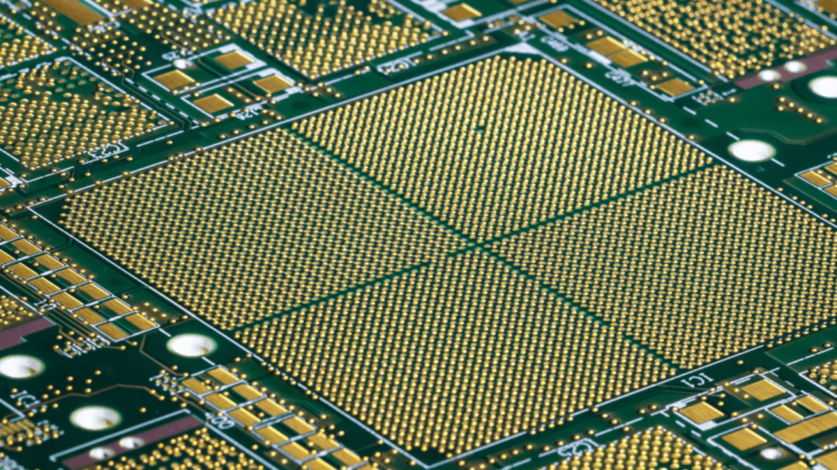
HDI refers to a technology allowing for the manufacture of PCBs with higher rounds densities and better lines and spaces than traditional methods. This advancement in PCB design involves the use of microvias, fine lines and spaces, and advanced layer stacking techniques to achieve greater functionality and miniaturization. Unlike conventional PCBs, which primarily utilize through-hole vias and larger track widths, HDI boards employ multiple layers of densely packed collections interconnected through microvias, enabling significant space savings and improved signal integrity.
Advancement and Advancements:
The development of HDI technology can be followed back to the increasing demand for smaller and more lightweight gadgets, particularly in industries such as consumer electronics, telecom, and medical devices. As gadgets became slighter, traditional PCB manufacturing techniques struggled to keep pace with the need for higher rounds densities and improved performance.
One of the key advancements in HDI technology is the using of laser drilling for creating microvias. Laser drilling offers unparalleled precision and control, making it possible for the creation of smaller diameter vias with higher aspect ratios. Additionally, advancements in materials science have led to the development of high-performance substrates and laminates capable of supporting the fine features and high-density routing required by HDI designs.
Applications Across Industries:
The versatility of HDI technology has made it imperative across a wide range of industries. In consumer electronics, HDI PCBs enable the development of ultra-thin smartphones one the market, capsules, and wearable devices without compromising on performance. The car industry utilizes HDI technology to integrate complex electronic systems into vehicles, including advanced driver-assistance systems (ADAS) and infotainment systems.
Moreover, HDI technology plays a vital role in aerospace and defense applications, where reliability and miniaturization are critical. Space-constrained medical devices, such as pacemakers and implantable sensors, benefit from the compact form factor and high reliability offered by HDI PCBs. The industrial sector also leverages HDI technology for automation, robotics, and IoT devices, where space optimization and robustness are paramount.
Recent Advancements and Innovations:
In recent years, the advancement of HDI technology has been propelled by innovations in manufacturing processes, materials, and design tools. Three-dimensional (3D) printing techniques have emerged as a promising approach for producing complex HDI structures with reduced lead times and costs. Component manufacturing enables the creation of intricate geometries and customized designs, opening up new possibilities for next-generation gadgets.
Furthermore, the integration of artificial learning ability (AI) and machine learning algorithms into the PCB design process has facilitated the optimization of HDI themes for improved signal integrity, winter management, and reliability. AI-driven design tools analyze vast amounts of data to spot optimal routing configurations, layer stackups, and via placements, increasing the development cycle and enhancing overall performance.
Future Trends and Outlook:
Looking ahead, the future of HDI technology is poised for continued growth and innovation. With the advent of 5G networks, Internet of Things (IoT) devices, and edge calculating applications, the demand for compact yet powerful electronic systems will only intensify. HDI technology is expected to play a pivotal role in meeting these demands by enabling the development of high-performance, miniaturized PCBs for a diverse selection of applications.
Moreover, the convergence of HDI technology with other emerging trends, such as flexible and stretchable electronic devices, bioelectronics, and quantum calculating, holds promise for groundbreaking advancements in electronic devices manufacturing. Flexible HDI substrates could revolutionize wearable electronic devices and conformal medical devices, while quantum-inspired routing algorithms could maximize interconnects in next-generation calculating systems.
In conclusion, High Thickness Interconnect (HDI) technology represents a cornerstone of modern electronic devices manufacturing, enabling the development of smaller, faster, and more reliable gadgets across industries. With ongoing advancements in materials, manufacturing processes, and design methodologies, HDI technology is poised to continue driving innovation and healthy diet the future of electronic devices for many years to come.